C0402C758C5GAC7867
| Model | C0402C758C5GAC7867 |
| Description | Ceramic Capacitor, Multilayer, Ceramic, 50V, 33.3333% +Tol, 33.3333% -Tol, C0G, -/+30ppm/Cel TC, 0.00000075uF, 0402 |
| PDF file | Total 19 pages (File size: 1011K) |
| Chip Manufacturer | KEMET |


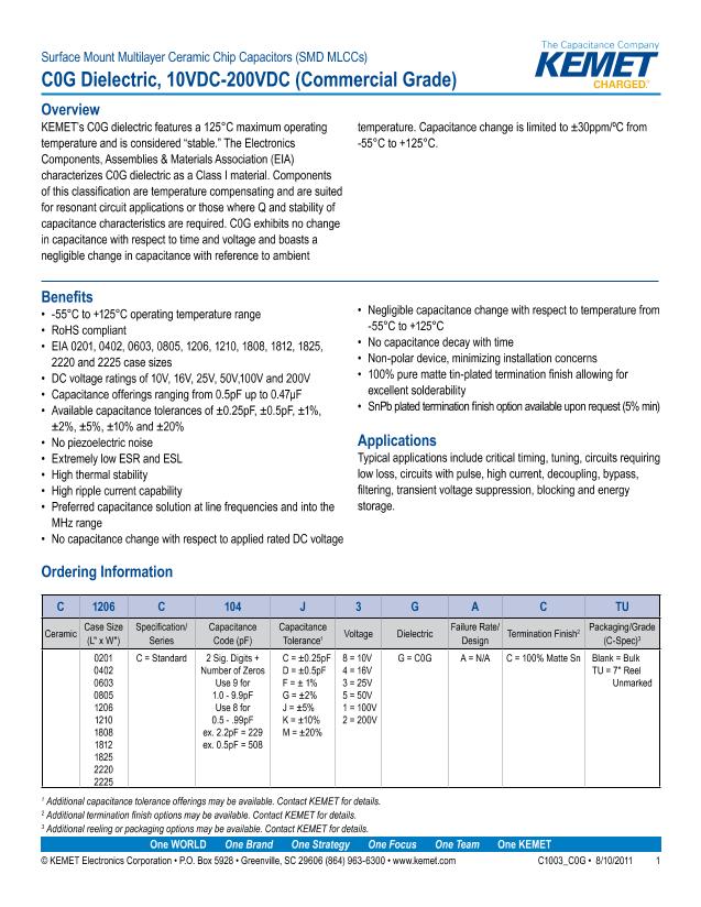
Surface Mount Multilayer Ceramic Chip Capacitors (SMD MLCCs) – C0G Dielectric, 10VDC-200VDC (Commercial Grade)
Table 2 – Chip Thickness/Packaging Quantities con’t
Thickness
Code
HG
JB
JC
JD
JE
JF
JP
JG
JH
JO
JP
JR
KB
KC
KD
KE
KF
Chip
Size
1825
2220
2220
2220
2220
2220
2220
2220
2220
2220
2220
2220
2225
2225
2225
2225
2225
Thickness ±
Range (mm)
1.60 ± 0.20
1.00 ± 0.15
1.10 ± 0.15
1.30 ± 0.15
1.40 ± 0.15
1.50 ± 0.15
1.60 ± 0.20
1.70 ± 0.15
1.80 ± 0.15
2.40 ± 0.15
3.50 ± 0.30
5.00 ± 0.50
1.00 ± 0.15
1.10 ± 0.15
1.30 ± 0.15
1.40 ± 0.15
1.60 ± 0.20
QTY per Reel QTY per Reel QTY per Reel QTY per Reel
7" Plastic
13" Plastic
7" Paper
13" Paper
1000
1000
1000
1000
1000
1000
1000
1000
1000
500
250
150
1000
1000
1000
1000
1000
4000
4000
4000
4000
4000
4000
4000
4000
4000
2000
850
600
4000
4000
4000
4000
4000
QTY per Bulk
Cassette
Thickness
Code
Chip
Size
Thickness ±
Range (mm)
QTY per Reel
7" Plastic
QTY per Reel
13" Plastic
QTY per Reel
7" Paper
QTY per Reel
13" Paper
QTY per Bulk
Cassette
Table 3 – Chip Capacitor Land Pattern Design Recommendations per IPC-7351
EIA
Size
Code
01005
0201
0402
0603
0805
1206
1210
1808
1812
1825
2220
2225
Metric
Size
Code
0402
0603
1005
1608
2012
3216
3225
4520
4532
4564
5650
5664
Density Level A:
Maximum (Most)
Land Protrusion (mm)
C
0.33
0.38
0.50
0.90
1.00
1.60
1.60
2.30
2.15
2.15
2.75
2.70
Y
0.46
0.56
0.72
1.15
1.35
1.35
1.35
1.75
1.60
1.60
1.70
1.70
X
0.43
0.52
0.72
1.10
1.55
1.90
2.80
2.30
3.60
6.90
5.50
6.90
V1
1.60
1.80
2.20
4.00
4.40
5.60
5.65
7.40
6.90
6.90
8.20
8.10
V2
0.90
1.00
1.20
2.10
2.60
2.90
3.80
3.30
4.60
7.90
6.50
7.90
C
0.28
0.33
0.45
0.80
0.90
1.50
1.50
2.20
2.05
2.05
2.65
2.60
Density Level B:
Median (Nominal)
Land Protrusion (mm)
Y
0.36
0.46
0.62
0.95
1.15
1.15
1.15
1.55
1.40
1.40
1.50
1.50
X
0.33
0.42
0.62
1.00
1.45
1.80
2.70
2.20
3.50
6.80
5.40
6.80
V1
1.30
1.50
1.90
3.10
3.50
4.70
4.70
6.50
6.00
6.00
7.30
7.20
V2
0.70
0.80
1.00
1.50
2.00
2.30
3.20
2.70
4.00
7.30
5.90
7.30
C
0.23
0.28
0.40
0.60
0.75
1.40
1.40
2.10
1.95
1.95
2.55
2.50
Density Level C:
Minimum (Least)
Land Protrusion (mm)
Y
0.26
0.36
0.52
0.75
0.95
0.95
0.95
1.35
1.20
1.20
1.30
1.30
X
0.23
0.32
0.52
0.90
1.35
1.70
2.60
2.10
3.40
6.70
5.30
6.70
V1
1.00
1.20
1.60
2.40
2.80
4.00
4.00
5.80
5.30
5.30
6.60
6.50
V2
0.50
0.60
0.80
1.20
1.70
2.00
2.90
2.40
3.70
7.00
5.60
7.00
Density Level A:
For low-density Product applications. Recommended for wave solder applications and provides a wider process window for reflow solder
processes. KEMET only recommends wave soldering of EIA 0603, 0805 and 1206 case sizes.
Density Level B:
For products with a moderate level of component density. Provides a robust solder attachment condition for reflow solder processes.
Density Level C:
For high component density product applications. Before adapting the minimum land pattern variations the user should perform qualification
testing based on the conditions outlined in IPC standard 7351 (IPC-7351).
© KEMET Electronics Corporation • P.O. Box 5928 • Greenville, SC 29606 (864) 963-6300 • www.kemet.com
C1003_C0G • 8/10/2011
8


