J201-E3
| Model | J201-E3 |
| Description | Small Signal Field-Effect Transistor, 1-Element, N-Channel, Silicon, Junction FET, TO-226AA, PLASTIC, TO-92, 3 PIN |
| PDF file | Total 6 pages (File size: 96K) |
| Chip Manufacturer | VISHAY |


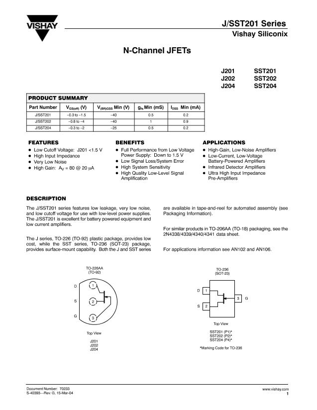
J/SST201 Series
Vishay Siliconix
TYPICAL CHARACTERISTICS (T
A
= 25_C UNLESS OTHERWISE NOTED)
500
Transfer Characteristics
V
GS(off)
=
−0.7
V
V
DS
= 10 V
2
Transfer Characteristics
V
GS(off)
=
−1.5
V
V
DS
= 10 V
400
I
D
−
Drain Current (mA)
I
D
−
Drain Current (mA)
1.6
T
A
=
−55_C
1.2
25_C
300
T
A
=
−55_C
25_C
200
125_C
100
0.8
0.4
125_C
0
0
−0.1
−0.2
−0.3
−0.4
−0.5
V
GS
−
Gate-Source Voltage (V)
0
0
−0.4
−0.8
−1.2
−1.6
−2
V
GS
−
Gate-Source Voltage (V)
1.5
g
fs
−
Forward Transconductance (mS)
Transconductance vs. Gate-Source Voltage
V
GS(off)
=
−0.7
V
V
DS
= 10 V
f = 1 kHz
4
g
fs
−
Forward Transconductance (mS)
Transconductance vs. Gate-Source Voltage
V
GS(off)
=
−1.5
V
V
DS
= 10 V
f = 1 kHz
1.2
T
A
=
−55_C
0.9
25_C
3.2
2.4
T
A
=
−55_C
25_C
0.6
125_C
0.3
1.6
0.8
125_C
0
0
0
−0.1
−0.2
−0.3
−0.4
−0.5
V
GS
−
Gate-Source Voltage (V)
0
−0.4
−0.8
−1.2
−1.6
−2
V
GS
−
Gate-Source Voltage (V)
200
Circuit Voltage Gain vs. Drain Current
g
fs
R
L
A
V
+
1
)
R g
L os
Assume V
DD
= 15 V, V
DS
= 5 V
R
L
+
10 V
I
D
r
DS(on)
−
Drain-Source On-Resistance (
Ω )
2000
On-Resistance vs. Drain Current
160
A
V
−
Voltage Gain
1600
V
GS(off)
=
−0.7
V
120
1200
80
−1.5
V
40
V
GS(off)
=
−0.7
V
800
−1.5
V
400
0
0.01
0.1
I
D
−
Drain Current (mA)
www.vishay.com
1
0
0.01
0.1
I
D
−
Drain Current (mA)
Document Number: 70233
S-40393—Rev. G, 15-Mar-04
1
4


