X1288V14-2.7A
| Model | X1288V14-2.7A |
| Description | 2-Wire RTC Real Time Clock/Calendar/CPU Supervisor with EEPROM |
| PDF file | Total 31 pages (File size: 559K) |
| Chip Manufacturer | XICOR |


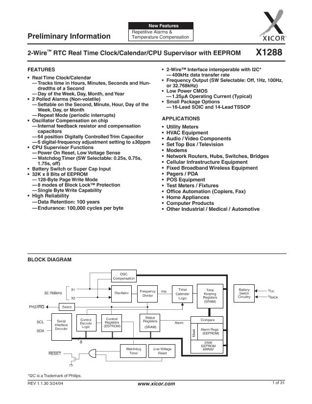
Preliminary Information
array the slave byte must be 1010111x in both
instances. Similarly, for a random read of the Clock/
Control Registers, the slave byte must be 1101111x in
both places.
Write Operations
Byte Write
For a write operation, the device requires the Slave
Address Byte and the Word Address Bytes. This gives
the master access to any one of the words in the array
or CCR. (Note: Prior to writing to the CCR, the master
must write a 02h, then 06h to the status register in two
preceding operations to enable the write operation.
See “Writing to the Clock/Control Registers.” Upon
receipt of each address byte, the X1288 responds with
an acknowledge. After receiving both address bytes
the X1288 awaits the eight bits of data. After receiving
the 8 data bits, the X1288 again responds with an
acknowledge. The master then terminates the transfer
by generating a stop condition. The X1288 then begins
an internal write cycle of the data to the nonvolatile
memory. During the internal write cycle, the device
inputs are disabled, so the device will not respond to
any requests from the master. The SDA output is at high
impedance. See Figure 12.
A write to a protected block of memory is ignored, but
will still receive an acknowledge. At the end of the write
command, the X1288 will not initiate an internal write
cycle, and will continue to ACK commands.
Figure 12. Byte Write Sequence
Signals from
the Master
S
t
a
r
t
1
S
t
o
p
X1288
Page Write
The X1288 has a page write operation. It is initiated in
the same manner as the byte write operation; but
instead of terminating the write cycle after the first data
byte is transferred, the master can transmit up to 127
more bytes to the memory array and up to 7 more
bytes to the clock/control registers. (Note: Prior to writ-
ing to the CCR, the master must write a 02h, then 06h
to the status register in two preceding operations to
enable the write operation. See “Writing to the Clock/
Control Registers.”
After the receipt of each byte, the X1288 responds with
an acknowledge, and the address is internally incre-
mented by one. When the counter reaches the end of
the page, it “rolls over” and goes back to the first
address on the same page. This means that the mas-
ter can write 128 bytes to a memory array page or 8
bytes to a CCR section starting at any location on that
page. For example, if the master begins writing at loca-
tion 105 of the memory and loads 30 bytes, then the
first 23 bytes are written to addresses 105 through
127, and the last 7 bytes are written to columns 0
through 6. Afterwards, the address counter would point
to location 7 on the page that was just written. If the
master supplies more than the maximum bytes in a
page, then the previously loaded data is over written by
the new data, one byte at a time. Refer to Figure 13.
The master terminates the Data Byte loading by issu-
ing a stop condition, which causes the X1288 to begin
the nonvolatile write cycle. As with the byte write oper-
Slave
Address
1 110
A
C
K
Word
Address 1
0
A
C
K
Word
Address 0
Data
SDA Bus
Signals From
The Slave
A
C
K
A
C
K
Figure 13. Writing
30
bytes to a
128-byte
memory page starting at address
105.
7 Bytes
23 Bytes
Address
=6
Address Pointer
Ends Here
Addr = 7
Address
105
Address
127
REV 1.1.30 3/24/04
www.xicor.com
21 of 31


