LV9720DEV-670.0M-T500
| Model | LV9720DEV-670.0M-T500 |
| Description | LVDS Output Clock Oscillator, 10.9MHz Min, 670MHz Max, 670MHz Nom, ROHS COMPLIANT, CERAMIC, SMD, 6 PIN |
| PDF file | Total 8 pages (File size: 319K) |
| Chip Manufacturer | PLETRONICS |


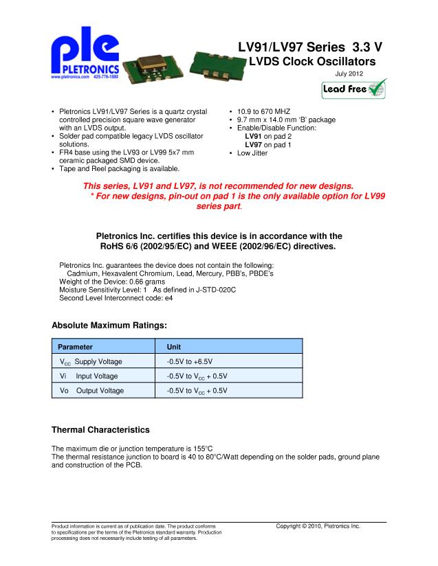
LV91/LV97 Series 3.3 V
LVDS Clock Oscillators
July 2012
Reliability
: Environmental Compliance
Parameter
Mechanical Shock
Vibration
Solderability
Thermal Shock
Condition
MIL-STD-883 Method 2002, Condition B
MIL-STD-883 Method 2007, Condition A
MIL-STD-883 Method 2003
MIL-STD-883 Method 1011, Condition A
ESD Rating
Model
Human Body Model
Charged Device Model
Minimum Voltage
1500
1000
Conditions
MIL-STD-883 Method 3115
JESD 22-C101
Package Labeling
Label is 1" x 2.6" (25.4mm x 66.7mm)
Font is Courier New
Bar code is 39-Full ASCII
(The part number will show as LV91xx or LV97xx)
Label is 1" x 2.6" (25.4mm x 66.7mm)
Font is Arial
Layout and application information
For Optimum Jitter Performance, Pletronics recommends:
•
a ground plane under the device
•
no large transient signals (both current and voltage) should be routed under the device
•
do not layout near a large magnetic field such as a high frequency switching power supply
•
do not place near piezoelectric buzzers or mechanical fans.
As much ground plane and thermal paths that can be realized under and to the side of the part is desired
.
www.pletronics.com
425-776-1880
5


