LV9720DEV-670.0M-T500
| Model | LV9720DEV-670.0M-T500 |
| Description | LVDS Output Clock Oscillator, 10.9MHz Min, 670MHz Max, 670MHz Nom, ROHS COMPLIANT, CERAMIC, SMD, 6 PIN |
| PDF file | Total 8 pages (File size: 319K) |
| Chip Manufacturer | PLETRONICS |


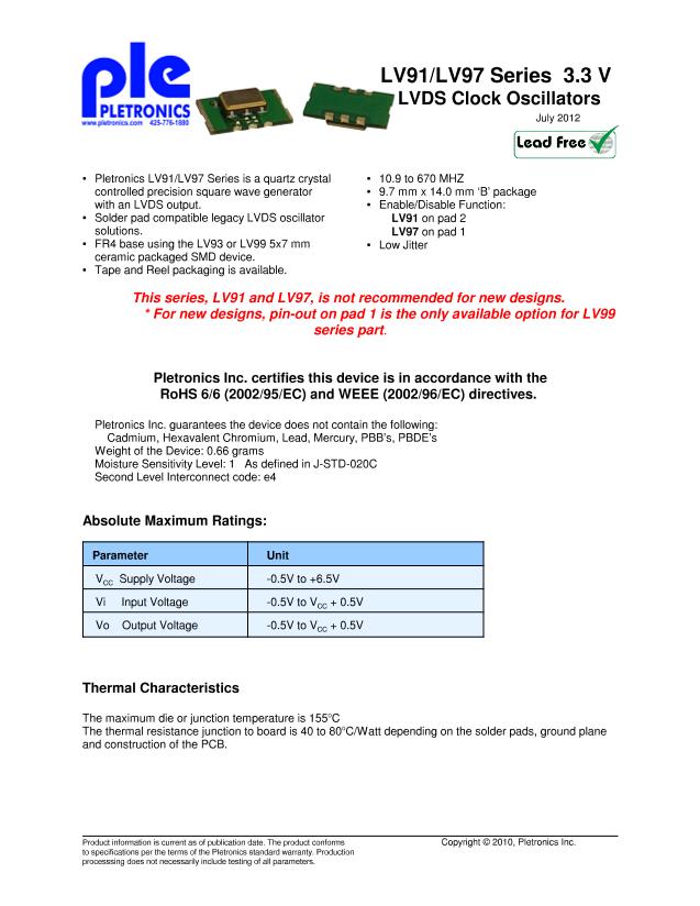
LV91/LV97 Series 3.3 V
LVDS Clock Oscillators
July 2012
Mechanical:
Inches
A
B
C
2
2
2
2
6
6
6
6
1
1
1
1
5
5
5
5
4
4
4
4
3
3
3
3
mm
9.65 +0.25
_
13.97 +0.25
_
2.49 +0.25
_
0.66
1.27
0.72 R
4.57
2.54
1.27
0.38
0.380 +0.010
_
0.550 +0.010
_
0.098 +0.010
_
0.026 typ.
0.050
0.028 R
0.180
0.100
0.050
0.015
1
D
1
E
1
F
1
G
1
FR4 PCB Base:
Solder masked
All via holes tented on bottom
Copper Clad �½ oz. Typical
Gold plated 0.02 µinch (0.5 µm)
Label:
Laser engraved on the 5x7 mm
oscillator that is mounted on the
FR4 base
Pin 3 Ground plane is typical
H
1
I
1
Not to scale
J
1
Typical Dimensions
LV91
Pad
2
LV97
Pad
1
Function
Note
Output
When this pad is not connected the oscillator shall operate. This is not a
Enable/Disable recommended condition!!!!!!
When this pad is <0.80 volts, the output will be inhibited (High impedance state)
Recommend connecting this pad to V
CC
if the oscillator is to be always on.
No function
Ground (GND)
Output
Output*
The outputs must be terminated, 100 ohms between the outputs is the ideal
termination.
Capacitor coupled terminations can be used.
Recommend connecting this pad to ground. The is internal connection.
1
3
4
5
6
2
Supply Voltage Recommend connecting appropriate power supply bypass capacitors as close as
(V
CC
)
possible.
www.pletronics.com
425-776-1880
6


