
W152-3GT
| Model | W152-3GT |
| Description | PLL Based Clock Driver, 8 True Output(s), 0 Inverted Output(s), PDSO16, 0.150 INCH, SOIC-16 |
| PDF file | Total 8 pages (File size: 146K) |
| Chip Manufacturer | CYPRESS |


W152
Spread Aware™, Eight Output Zero Delay Buffer
Features
• Spread Aware™—designed to work with SSFTG
reference signals
• Two banks of four outputs each
• Configuration options to halve, double, or quadruple
the reference frequency refer to
Table 1
to determine
the specific option which meets your multiplication
needs
• Outputs may be three-stated
• Available in 16-pin SOIC package
• Extra strength output drive available (-11/-12 versions)
• Contact factory for availability information on 16-pin
TSSOP
Output to Output Skew: Between Banks .....................215 ps
Output to Output Skew: Within Banks
(Refer to
Figure 4)
...................................................100 ps
Total Timing Budget Impact: ........................................555 ps
Max. Phase Error Variation:.......................................±225 ps
Tracking Skew: ..........................................................±130 ps
Table 1. Configuration Options
Device
W152-1/11
[1]
Feedback Signal
QA0:3 or QB0:3
QA0:3
QB0:3
QA0:3
QB0:3
QA0:3 or QB0:3
QA0:3
REFx1
REFx1
REFx2
REFx2
REFx4
REFx2
QB0:3
REFx1
REF/2
REFx1
REFx1
REFx2
REFx2
W152-2/12
[2]
W152-2/12
[2]
W152-3
W152-3
W152-4
Key Specifications
Operating Voltage: ............................................... 3.3V±10%
Operating Range: ................... 15 MHz < f
OUTQA
< 140 MHz
Cycle-to-Cycle Jitter: (Refer to
Figure 3)
.................... 225 ps
Cycle-to-Cycle Jitter: Frequency Range
25 to140 MHz ......................................................... 125 ps
Notes:
1. W152-11 has stronger output drive than the W152-1.
2. W152-12 has stronger output drive than the W152-2.
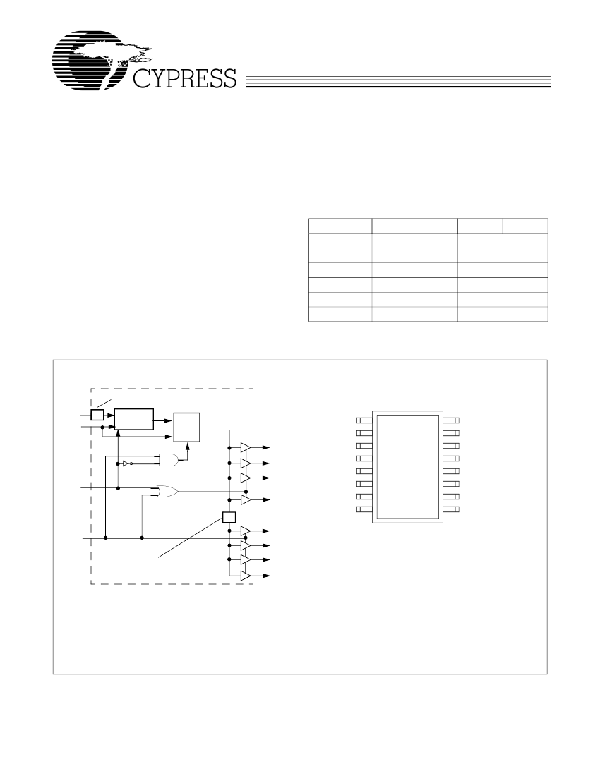
Block Diagram
(present on the -3 and -4 only)
Pin Configuration
FBIN
REF
÷2
PLL
MUX
QA0
QA1
QA2
REF
QA0
QA1
VDD
GND
QB0
QB1
SEL1
QB0
QB1
1
2
3
4
5
6
7
8
16
15
14
13
12
11
10
9
FBIN
QA3
QA2
VDD
GND
QB3
QB2
SEL0
SEL0
QA3
÷2
SEL1
(present on the -2, -12, and -3 only)
QB2
QB3
Spread Aware is a trademark of Cypress Semiconductor Corporation.
Cypress Semiconductor Corporation
Document #: 38-07148 Rev. *A
•
3901 North First Street
•
San Jose
•
CA 95134 • 408-943-2600
Revised December 14, 02


