Design and Implementation of DVB-C Set-top Box Source Decoder
Summary: This paper implements a set-top box source decoder with SC2005 as the main chip, and connects the decoder with L64768 front-end to form a complete set-top box scheme conforming to DVB-C standard. It can decode audio and video streams conforming to the MPEG-2 standard and is compatible with PAL/NTSC/SECAM analog TV reception.
Introduction
In recent years, the development of digital radio and TV in China has been significantly accelerated, which has directly triggered a huge market demand for Set-top Box, highlighting its importance. In the research and development process of set-top box, the development of source decoder is the basis of the whole development work. With the introduction of the card separation policy, the universality and complexity of the source decoder make it more important in the development of set-top box terminals. This paper discusses the design and implementation of DVB-C compliant source decoder for digital cable set-top box.
Overall scheme
Set-top boxes can generally be divided into two functional parts: channel demodulation and decoding and source decoding. The channel part, the front-end, is responsible for demodulating, receiving and decoding digital TV signals. Due to the different front-end, set-top boxes can be divided into digital satellite set-top boxes, digital terrestrial set-top boxes and digital cable set-top boxes.
The source decoder is developed for the digital cable set-top box. It will be connected with the L64768 front-end to form a complete set-top box scheme conforming to the DVB-C standard. This paper uses LSI Logic's SC2005-based second-generation monolithic source decoding scheme to achieve decoding function. The structure diagram of the decoder is shown in Figure 1. It can be divided into four parts by function: CPU with SC2005 and storage control subsystem. Transmit stream demultiplexing and audio-video decoding subsystem; Graphics processing and screen menu display and output subsystem; Peripheral interface subsystem.
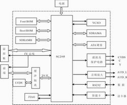
Figure 1 Set-top box source decoder
Hardware implementation
The source decoder's startup code is stored in the Flash Boot ROM, and the font used is stored in the Flash Font ROM. Two SDRAMs for SC2005storageThe interfaces are connected to SDRAM-A and SDRAM-B, respectively. After the system is powered up, the startup code saved in the Flash Boot ROM is transferred to SDRAM-B for execution. Clock controlled by 27MHz voltageoscillatorProvided after frequency doubling.Voltage controlled oscillatorThe generated clock signal is reshaped by 74LVC14 and sent to the VCXO pin of SC2005, which is synchronously restored by the output of the SDET pin. Transport stream multiplexing, audio/video decoding, graphics processing and other functions are integrated by SC2005.ModularIt is implemented with external related circuits.
CPU and Storage Control Subsystem
SC2005 integrates the functions of transport demultiplexer L641x8 and MPEG-2 audio-video decoder L64105. It contains EZ4102 core, 16KB instruction Cache and 8KB data Cache, which are the components of SC2005.
Two 1M slices for this source decoder × 16bit Flash ROMs are all AM29LV160DT-70, using a singlePower SupplyPower supply, read-write and programming all use 3.3V voltage, high speed 70ns read-write time. They are connected to SC2005 through E-Bus, ADDR[7:1] for Address Bus A[6:0] and SC2005, AD[28:16] for A[19:7] and SC2005, and AD[15:0] for Data Bus DQ[15:0] and SC2005. There are 35 sectors in the chip, four of which are the guide sectors, ranging in size from 4K to 16K words, and the remaining 31 sectors are 32K words. There is a byte/word mode selection pin BYTE#. In this design, the pin connects to a high level, and the word mode is selected.
81MHz/1M × 16bit SDRAM-A and 108MHz/2M × 16 bit S DRAM-B is connected to the S DRAM memory interface of the CPU through S-BUS. SDRAM-A is used to store video frames and related information when decoding MPEG, and SDRAM-B stores information of demultiplexing, OSG and peripheral device interface subsystems. SDRAM-A and SDRAM-B can transfer data directly through a DMA engine.
Transmit Stream Demultiplexing and Audio Video Decoding Subsystem
SC2005 first receives TS streams from channel decoders or code stream generators, and then automatically performs packet synchronization detection. Once synchronization is established, the transport package is sent to the PID preprocessor. The PID preprocessor analyzes the input packets and checks their PID values. Only the PID values that match the PID table can be filtered step by step, and the unmatched packets are discarded. Through PIDWave filterThe transport package is sent to the DVB decoder, the decoded package enters the PID post-processor, the audio-video PES data enters the A/V decoder directly after filtering, and the other data is sent to the circular buffer of the external SDRAM-B, and the CPU can read the data directly from the memory. The structure diagram of the transport stream demultiplexing subsystem is shown in Figure 2.

Figure 2 Transport stream demultiplexing subsystem
The demultiplexed audio-video PES stream enters the L64105 MPEG-2 decoder through the A/V interface for block decoding. L64105 outputs two groups of digital video and digital audio signals. A set of digital video and a set of digital audio signals are output directly. Another set of digital video signals is sent to a video encoder and converted to a full-TV signal (CVBS) or SterminalSignal (Y/C), after external low-pass filtering, is directly sent to the TV; Digital audio signals are sent to the audio DAC, converted into stereo analog signals, and output after external low-pass filtering.
Graphics Processing and Screen Menu Display Output Subsystem
SC2005 integrates a high-performance OSG (On-Screen Graphics) subsystem that generates text and graphics and superimposes them on decoded video. OSG subsystem produces static layer, OSD layer and cursor layer. The decoding subsystem provides the video layer; The Mixer/Encoder subsystem generates a background color layer and encodes the above five layers before video output to display the desired output composite video. This subsystem mixes graphics and decoded video data from the OSG subsystem and outputs RGB/YPbPr, CVBS or S video signals in NTSC/PAL/SECAM format to the TV or monitor.

Figure 3 ATA Hard Disk Interface
Peripheral Interface Subsystem
The source decoder integrates an ATA hard disk interface as shown in Figure 3. The user can realize the PVR (Personal Video Recorder) function of the personal digital video recorder through this interface. You can also open a large cache on your hard disk to store your programs in real time for hours while playing digital TV. Depending on this caching technology, users can play time-lapse.
The decoder has a TDA8004T smart card interface and a JTAG module compliant with the IEEE 1149.1 standard, provides basic debugging functions, and provides an LVDS interface to receive TS streams from the code stream generator. The LVDS signal input by DB-25 interface passes through three DS90C032 slices for level transformation and enters the decoder. In addition, the system uses a UART for set-top box debugging and software upgrade.

Figure 4 Set-top Box Software Layered Framework
software design
The software system is based on a hierarchical framework, in which some parts are provided by LSI Logic in its reference software and others are developed by users themselves. The overall structure of the software is shown in Figure 4.
The Real-time Operating System Layer (RTOS) is the basis for all the upper program code running. It is mainly responsible for multitask scheduling, system resource management, interrupt processing, communication operations and synchronization processing. This paper uses a modular, high performance real-time operating system, pSOSystem, designed and developed by WindRiver for embedded systems. The RTOS layer uses a board-level support package (BSP) to interface with the hardware layer.
The Operating System Porting Layer (OSP) implements two main functions: one is to dynamically configure the properties of tasks, such as context switching, priority, etc. Another is to manage communication between tasks, such as data transfer and synchronization. Hardware Abstraction Layer (HAL) is responsible for programming hardware registers directly; The Device Driver Layer (DDL) is a clear and convenient backup of the hardware abstraction layer andencapsulationIt mainly provides drivers for each hardware module, such as SC2005 exception handling driver, clock service module driver and OSG graphics library driver. Application Interface Layer (API) provides API functions for upper-level applications.
Driver Adaptation Layer (DAL) is a further collection of device driver layer functions that can be applied directly to the application layer through a combination of functions, and it acts as an interface. For example, operations on Flash can be further encapsulated with such a driver adapter layer to facilitate calls from upper applications.
The user application layer is the main part of the set-top box user application software and the focus of software development. All the top-level functions related to the set-top box are implemented in this layer, such as the implementation of user interface functions, EPG implementation, program database management, user information input/output control and software upgrade.
Source:Xiang Xueqin
Copyright & Disclaimer
All works on this website that state "Source: ICMoment", all copyright belongs to ICMoment, please
specify
icmoment, https://www.icmoment.com, violators will be investigated for related The website will be held
legally responsible.
This website reproduces and indicates works from other sources, the purpose is to pass on more
information,
does not mean that the network agrees with its views or to confirm the authenticity of its content, does
not
assume direct responsibility for such works of infringement and joint and several liability. When other
media, websites or individuals reprint from this website, they must retain the source of the work
indicated
on this website and bear their own legal responsibility for copyright and other issues.
If the content of the work, copyright and other issues are involved, please contact us within one week from the date of publication of the work, otherwise it is regarded as a waiver of the relevant rights.
Related Readings
Popular Circuit Diagrams
Special Sale
Model
Price
