Design of Video Controller in H.264 Video Decoding Chip
Introduction
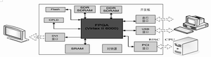
H.264 is a new video compression standard jointly studied by ITU-T VCEG and ISO/IEC MPEG. Compared with other video compression algorithms, H.264 has the characteristics of high compression ratio and complex algorithm. Because of the complexity of the encoding algorithm, the system requires very strict image decoding speed and power consumption. Therefore, the H.264 decoding chip is used in the design of the decoder. For a large design project, the top-down (TOP-DOWM) design method is generally used to divide each module into sub-modules. The video controller module is the data interface between the chip and the display platform. It plays an important role in verifying the success of the chip design. It is necessary to divide the module into a separate sub-module. In order to improve the success rate of the design, the prototype verification based on GA was used at the beginning of the design. As shown in Fig. 1, the platform is divided into two parts, hardware design and software decoding based on RISC CPU. The two parts work together to verify the decoding results of both software and hardware, and to speed up the whole decoding process.
 & Nbsp;
Figure 1 A prototype verification platform for a H.264 decoding chip based on a GA
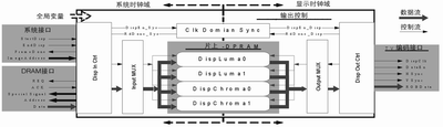
Figure 2 Output video control module block diagram
Design and implementation of video control module
Principle block diagram and function analysis of video control module
The structure diagram of the output video control module is shown in Figure 2, which has two clock domains: the system clock domain and the display clock domain. The system clock frequency is fixed at 166MHz according to the selected SDRAM type. For resolution 1280 × For 720 HDTV, the display clock domain can select a frequency of around 70 MHz.
The system clock domain contains two external interfaces: the system interface, which mainly contains the instructions issued by the upper system and the feedback information of the output control module. The DRAM interface, which contains the signal provided by the data private bus to the output control module for requesting image data for display from DRAM.
The Display Input Control Submodule (Disp In Ctrl) in the system clock domain is used to receive the StartDisp and EndDisp signals from the system first to start or turn off the output display function of video data, and at the same time to issue the FrameDone signal to inform the system to change the address information of the next image (ImageAddress); Second, it is used to make requests to DRAM to read image data that needs to be displayed through a dedicated data channel. It also controls the Input MUX, which accomplishes the task of writing data to in-chip SRAM; To interact with information in the display clock domain, this module sends a DispEn Sys signal to the Clock Domain Sync module to control the opening and closing of image display. Another sub-module of the system clock field, the input multiple selection module, will select in-chip dual-port SRAM according to certain rules, control the memory address, and complete the task of writing display image data to the memory.
The display clock field contains an external display device interface, which mainly contains control signals for display and data information that has been converted. The display clock field consists of two sub-modules, one is Output MUX, which is used to select and control the address of double-port SRAM, and reads the image data to be displayed according to certain rules. Data is also packaged. Another sub-module is the Display Out Control Module (Disp Out Ctrl), which is used to control the TV encoder, convert YUV signal to RGB signal, and zoom the digital image, including display clock, line synchronization, frame synchronization and RGB image data. It also controls the output multiple selection module to read the display data; It interacts with the system clock domain to coordinate data transfer between the two clock domains.
Special technology used in video control module
The clock domain synchronization module is the focus of the output control module design. It is mainly responsible for the control signal transmission between two clock domains. The design of signal transmission across the clock domain is cumbersome, so there are two kinds of signals in the design: data signal and control signal, in which the control signal is transmitted through the clock domain synchronization module. To simplify the number of signals that need to be transmitted across the clock domain, only two signals are needed in the scheme: the WrDone signal is sent by the system clock domain, which informs the display that the data in a double-port SRAM in the clock domain has been updated and can be read and displayed as output; The RdDone signal is sent from the display clock field to inform the system that the data in a double-port SRAM in the clock field has been displayed and the internal data can be updated. Signal transmission between different clock domains requires the elimination of metastability, which allows the signal to be locked out through two levels of registers, as shown in Figure 3.
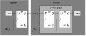
Figure 3 Cross-clock domain signal metastable cancellation circuit
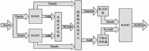
Figure 4 Hardware implementation block diagram of video output submodule
There are two points worth noting in the design. First, the clock domain synchronization circuit should be placed in a separate module to ensure the optimization of comprehensive tools, correct time series analysis, and convenient for circuit analysis and debugging. At the same time, in order to enable the target clock domain of the signal to collect signal changes, the control signals transmitted in the design are characterized by level signals.
Another type of signal to be transmitted between clock domains is data signals, which are transmitted through dual-port DPRAM because of the large number and fast change of data signals. Dual-port DPRAM requires reading and writing ports to operate on the same storage address at a certain time interval. Otherwise, data transmission errors may occur and even the hardware circuit may be damaged. Therefore, in order to avoid read-write conflict of DPRAM, a "ping-pong" buffer method is used in the design. Two pieces of DPRAM are accessed and decoded alternately to display brightness or color difference data. When the display part reads data from one DPRAM, the system writes the next data to another DPRAM, and when the data is read, the two pieces of DPRAM are exchanged. This part is implemented by 4 blocks of DPRAM, 2 blocks transmit brightness signals and 2 blocks transmit color difference signals.
Following is an analysis of the format conversion algorithms, image scaling algorithms, and their hardware implementations used in the video controller display output sub-module.
Display data format conversion analysis
According to the data of Sil 164 DVI signal encoding chip and the YUV_RGB conversion format given in H.264 video encoding standard, the fixed conversion algorithm used in the design is as follows: & Nbsp;
![]()
The above format is fixed-point processed and converted using shift and addition as follows:
![]()
In hardware design, YUV and RGB signals are all represented by 8-bit unsigned numbers, and intermediate variables are guaranteed by 12-bit. To clip the calculated RGB results in the range of 0 to 255, the power exponent and division operations in the formula are implemented by shifting.
Algorithmic Analysis of Digital Image Scaling
For a resolution of M × The original image of N whose YUV values at all sample points can be used with M × The N-order matrix is expressed as:
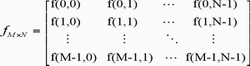
Pixel points are represented by f(m, n), where 0 < m < M and 0 < n. Scaling a digital image is essentially resampling a digital image. Assuming that the scaling multiples for the height and width of the original digital image are S1 and S2, according to Nyquist sampling law, a new horizontal and vertical sampling period of 740) this.width=740 "border=" undefined "> resampling the original digital image. The scaled digital image f'(m', n'):
![]()
As can be seen from the above formula, each reconstructed pixel F'(m', n') in the scaled digital image is the weighting of each pixel in the original digital image. If this type of hardware design is used directly, the amount of calculation will be very large. In order to simplify the design difficulty and save the cost of the chip, the above can be simplified on the basis of little influence on image quality. The reconstructed image pixel value mainly depends on the product of two sampling functions. Only used in practice![]() A point whose value is equal to 1 is the point satisfied. Further simplification is preferable, meaning that logarithms are rounded to obtain a simplified expression: f'(m', n')=f(m, n).
A point whose value is equal to 1 is the point satisfied. Further simplification is preferable, meaning that logarithms are rounded to obtain a simplified expression: f'(m', n')=f(m, n).
Hardware implementation of digital image format conversion and scaling
The display device was designed with a resolution of 1280 × 720 High Definition TV, output to High Definition TV display using image center alignment. When the decoded digital image data is sent to a high definition TV display, if it is not scaled, the decoded digital image is scaled in the middle of the display screen, and the rest is filled with black. When zooming, follow the rules above. The front end of the video controller output module is converted into data format according to the progressive scan arrangement of the incoming data, and then the pixel data with RGB not zero (i.e. not black) is placed in two equal-sized in-picture cache RAMs in turn according to the rule of each frame and progressive scan, as shown in Figure 4.
It works in the same way as the previous DPRAM. After reading the address of the data in RAM1 or RAM2, you can get the row and column address of the pixel value of the point through the address decoder, that is, the value of M and n. Send m and N values to the image zoom processing unit, get new image data and new image data address by zoom processing, and get address in output RAM3 in progressive scan format by writing address decoder, which is used to store format converted data. From RAM3 where converted data is stored, the RGB data needed for display can be directly output.
epilogue
After the design is completed, this video controller module is synthesized with the Synplify 7.6 tool to get 80.3MHz operating frequency. Downloaded with the front-end decoding module into Xilinx's Virtex-II 6000 type GA, and integrated into the H.264 video decoding verification platform, the working frequency can reach 34MHz, and the image can play well on high-definition TV.
Source:Xiang Xueqin
Copyright & Disclaimer
All works on this website that state "Source: ICMoment", all copyright belongs to ICMoment, please
specify
icmoment, https://www.icmoment.com, violators will be investigated for related The website will be held
legally responsible.
This website reproduces and indicates works from other sources, the purpose is to pass on more
information,
does not mean that the network agrees with its views or to confirm the authenticity of its content, does
not
assume direct responsibility for such works of infringement and joint and several liability. When other
media, websites or individuals reprint from this website, they must retain the source of the work
indicated
on this website and bear their own legal responsibility for copyright and other issues.
If the content of the work, copyright and other issues are involved, please contact us within one week from the date of publication of the work, otherwise it is regarded as a waiver of the relevant rights.
Related Readings
Popular Circuit Diagrams
Special Sale
Model
Price
