RF Power MOSFET Product and Process Development
The output power of power amplifier in mobile phone base station ranges from 5W to over 250W. RF power MOSFET is a cost component in mobile phone base station. The cost of the RF part in a typical mobile base station is about 65,000 US dollars, with the cost of the power amplifier reaching 40,000 US dollars. The annual sales of power amplifier components are about $800 million. With the development of 3G, the demand of RF power amplifier will be further improved.
RF power MOSFET is also used in the field of radio communication. Its frequency has been extended to low microwave band and its output power can exceed 100W. It is also used in power amplifiers, radar systems and military communications for television (especially digital TV).
With the rapid development and wider application of new generation wireless communication technology, RF power MOSFET has a very optimistic market prospects. At present, the RF power devices used in China are still dependent on imports, and less than 1% of the domestic RF chips and devices have their own products. Therefore, it is very important to develop RF power MOSFET independently.
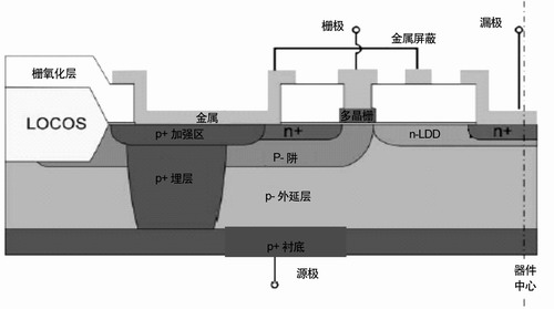
Figure 1 Basic structure diagram of LDMOSFET
RF Power LDMOSFET Performance Characteristics
Compared with silicon bipolar transistors, RF power LDMOSFET has the following advantages:
1. Higher frequency and good stability: Bipolar transistors can only operate in frequencies below 300 MHz, while LDMOSFET can operate in frequencies from several hundred MHz to several GHz due to its small feedback capacitance and good frequency stability.
2. High gain: Typically at the same output power level, bipolar transistors gain 8dB~9dB, while LDMOSFETs can reach 14dB.
3. Good linearity and low distortion: LDMOSFET performance is especially prominent in digital signal transmission applications.
4. Good thermal stability: Temperature has negative feedback effect on LDMOSFET current, and higher temperature can limit further increase of current; The temperature of the bipolar transistor has a positive feedback effect on the current, so the LDMOSFET has good thermal stability.
Basic Structure and Manufacturing Process Characteristics of RF Power LDMOSFET
RF power LDMOSFET is a power MOSFET with transverse channel structure. It uses LDMOSFET as its basic structure, uses double diffusion technology to diffuse boron and phosphorus in the same window successively, and controls the channel length by the difference of the junction depth of the transverse diffusion of the two impurities. Its basic structure, shown in Figure 1, consists of several key structures:
1. P+ Substrate and P-Epitaxial Layer: Devices generally use P+ Silicon Substrate with a P-Epitaxial Layer of a certain thickness, and P+ Substrate is used for the source to pull out well from the back; The P-epitaxy layer is designed to increase the source leakage breakdown voltage of the device.
2. P-traps, N+ sources/leaks, gate oxygen and polycrystalline grids: These are the basic elements that make up the MOS structure, and P-traps and N+ sources are formed by self-aligned injection and double diffusion techniques. P-well and N+ source injections diffuse laterally below the polycrystals, forming the channel and source region of the MOS.
3. LDD structure: From the edge of the grid to the drain end is a lightly doped LDD (Lightly Doped Drain) region that can withstand high voltage between source and drain. By optimizing the charge and length of the LDD region, the through voltage of the source and drain can be reached. Generally speaking, when the charge density in the LDD region is about 1011 cm-2~1013 cm-2, the source leakage through voltage can be obtained.
4. P+ Substrate: Connect the surface source and P+ Substrate, and the working current flows from the surface source to the P+ Substrate through the P+ Substrate and from the back. This eliminates the need for additional pull-out from the front lead, reduces the feedback capacitance inductance, and improves the frequency characteristics.
5. P+ enhancement zone and shield: P+ enhancement zone is to ensure that current flows from the source end of the surface to the P+ buried layer through the metal. The metal shielding structure is designed to reduce the voltage of the polycrystalline grid against the edge of the LDD region and prevent the thermal electron injection effect.
Difficulty Analysis and Solution of Product Design
By analyzing the performance and structure characteristics of RF power MOSFET device, the basic structure of the device is designed, and the key parameters are obtained through process and device simulation.
Key parameters of the device include:
1. Gate Oxygen Thickness: A suitable gate Oxygen Thickness should be designed according to the threshold voltage of the device, etc.
2. Channel length, impurity concentration and distribution: they determine the on-off voltage of the device and the through voltage between source and drain, which must be specially designed.
3. LDD Length and Impurity Concentration: The source-leak voltage of the shared portion of the LDD region, its length and distribution of impurity concentration must be optimized so that the breakdown voltage of the device can reach the value and the voltage distribution in the LDD region is even.
4. Epitaxy thickness and impurity concentration: They determine the longitudinal pass-through voltage between the N+ leak and the source coming from the substrate.
With the 6 inch chip production line, the RF power MOSFET manufacturing process is designed, including P+ buried layer, LOCOS, grid structure, P trap, source leakage and LDD structure, as well as contact hole, aluminum, passive layer.
The process difficulties and solutions are as follows:
1. Grid structure: A special grid structure and process manufacturing process are designed to meet the functional and frequency characteristics of the device.
2. Self-aligned injection and double-diffusion processes for P-trap and N+ source regions: Device channels are formed by the difference of the transverse diffusion of boron and phosphorus during the P-trap and N+ source region promotion. The two regions are formed by two self-aligned injection of polycrystals. The injection and push processes need to be strictly controlled.
3. P+ Trap Channel: The concentration and length of impurities in this area are the key factors determining the performance of the device. The injection and promotion processes must be strictly controlled in the manufacturing process to ensure the basic performance and uniformity of the device.
epilogue
By analyzing the performance and structure characteristics of RF power LDMOSFET, the structure of RF power LDMOSFET device is designed, the key parameters are determined by process and device simulation, and a set of manufacturing process flow matching the 6 inch chip production line is designed, and solutions to the difficulties in the process are presented.
Source:Xiang Xueqin
Copyright & Disclaimer
All works on this website that state "Source: ICMoment", all copyright belongs to ICMoment, please
specify
icmoment, https://www.icmoment.com, violators will be investigated for related The website will be held
legally responsible.
This website reproduces and indicates works from other sources, the purpose is to pass on more
information,
does not mean that the network agrees with its views or to confirm the authenticity of its content, does
not
assume direct responsibility for such works of infringement and joint and several liability. When other
media, websites or individuals reprint from this website, they must retain the source of the work
indicated
on this website and bear their own legal responsibility for copyright and other issues.
If the content of the work, copyright and other issues are involved, please contact us within one week from the date of publication of the work, otherwise it is regarded as a waiver of the relevant rights.
Related Readings
Popular Circuit Diagrams
Special Sale
Model
Price
