Exploring Output Ripple in a Negative Voltage Charge Pump Using LTspice
In this article, we’ll use LTspice simulations to more thoroughly understand output-voltage ripple and consider techniques for mitigating it within a charge pump circuit.
In a previous article, we investigated the effects of decreasing the load resistance—or, equivalently, increasing load current—on the performance of the negative voltage-generating switched-capacitor circuit shown in Figure 1.
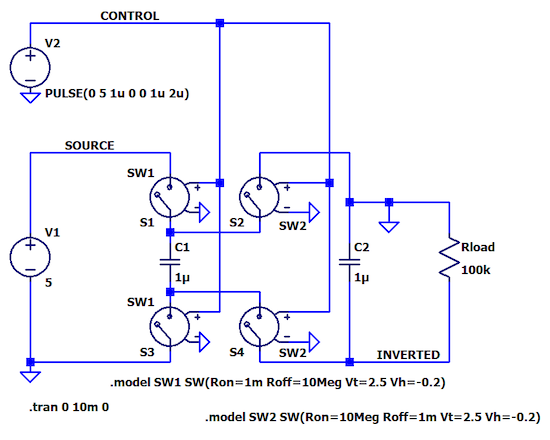
Figure 1. Diagram of a negative voltage-generating switched capacitor circuit.
Our simulation results demonstrated that decreased load resistance leads to a lower output-voltage magnitude and higher output-voltage ripple (Figure 2).
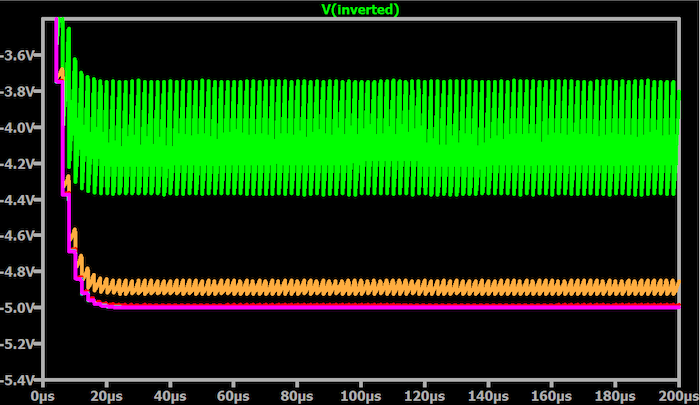
Figure 2. Plot showing the output voltage for RLOAD ranging from 100 kΩ (the magenta trace) to 10 Ω (the green trace).
As you can see, decreasing the load resistance eventually causes severe output ripple. With RLOAD = 10 Ω, the average value of the output voltage is around 4 V. Quite a few applications might tolerate a one-volt drop in VOUT, but I’m not sure how many would tolerate ~600 mV peak-to-peak ripple. If nothing else, we would expect analog components to couple significant amounts of noise from the power rail to their output signals.
Explaining Output Ripple Causes
First, let’s discuss what causes the output ripple. Lower load resistance equates to higher load current. If the load is drawing more current, C2 discharges—and therefore loses voltage—more quickly. Discharge/recharge behavior is inherent in the charge pump’s method of generating an output voltage; however, with small load currents, very little discharge occurs, and the discharge/recharge behavior is negligible. As the load current increases, the discharge/recharge cycles become more pronounced.
The next plot, Figure 3, shows VOUT for four different values of RLOAD (300 Ω, 100 Ω, 70 Ω, and 40 Ω).

Figure 3. Square wave plot showing the ripple frequency.
Using the above figure, you can confirm that the ripple frequency is the same regardless of load resistance. Furthermore, the ripple frequency is—as expected—the same as the frequency of the square wave that controls the switches.
Reducing Output Ripple—ESR, Output Capacitance, & Switch Control Frequency
Let’s rerun this simulation with just one value of load resistance. We’ll use a moderate value—say, 200 Ω. This corresponds to about 25 mA of load current, which is enough to power a few analog components and drive a bit of current into external circuitry.
As shown in the plot in Figure 4, we have ~37 mV peak-to-peak ripple.
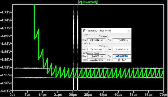
Figure 4. A plot showing a peak-to-peak ripple of ~37 mV.
Equivalent Series Resistance (ESR)
If I make one small change to our example circuit and run a new simulation, we can obtain these results, shown in Figure 5.
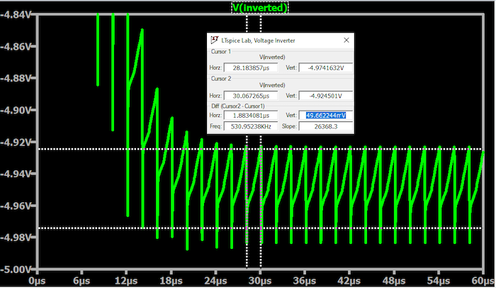
Figure 5. Plot showing the ripple increased over 50 mV by entering a value of 50 mΩ for the ESR of C2.
The ripple has increased to over 50 mV, and in fact, the measurement would be even worse if the cursor extended to the bottom of the sharp spike on the negative side of the waveform. What happened? Showing you my modified schematic won’t help because it looks exactly the same. All I did is insert a value of 50 mΩ for the equivalent series resistance (ESR) of C2, which can be seen in Figure 6.

Figure 6. Changing the ESR of C2 to 50 mΩ.
This indicates one way—a rather simple way, I’m glad to report—to reduce output ripple is choosing a capacitor with low ESR. It turns out that ripple magnitude in a circuit like this one is linearly proportional to the ESR of the output capacitor, so it’s definitely worth your time to take a close look at ESR specs if you’re concerned about output ripple.
Output Capacitance
You can also reduce ripple by increasing the output capacitance. Figure 7 shows a simulation with C2 = 3 μF (and with the ESR value removed).

Figure 7. A simulation plot with C2 = 3 μF and with the ESR value removed.
In this figure, the ripple has decreased from 37 mV to 13 mV, which indicates that a factor-of-three increase in output capacitance gives us an approximately factor-of-three reduction in output-voltage ripple. This result is consistent with the circuit’s theoretical model for ripple amplitude.
As usual, there is a trade-off here since higher capacitance may lead to a larger component or higher cost. Note that I say “may lead” because at low purchase quantities, a moderate increase in capacitance often will not affect the price of the component, even with the same package size.
Switch Control Frequency
The frequency of the square wave that controls the switches (fOSC) is another variable that influences ripple amplitude: you can reduce ripple by increasing fOSC. However, increasing the oscillator frequency simply to mitigate output ripple may not be a great idea because fOSC has additional important effects on the charge-pump circuit and on other components in the system. We’ll take a closer look at fOSC in a future article.
Reducing Output Ripple in a Switched-Capacitor Circuit
Output ripple is a key parameter in power-supply circuits; this applies not only to capacitor-based charge pumps but also to inductor-based switching regulators. In this article, we considered three methods of reducing ripple in a switched-capacitor power supply. Before we conclude, I’ll mention one more: you can use a linear voltage regulator to further regulate and filter the output supply (this is equally helpful with inductor-based switchers). It’s a highly effective and relatively simple strategy, but it requires additional cost and component area.
We’ll continue working with the LTspice charge pump in the next article.
Copyright & Disclaimer
All works on this website that state "Source: ICMoment", all copyright belongs to ICMoment, please
specify
icmoment, https://www.icmoment.com, violators will be investigated for related The website will be held
legally responsible.
This website reproduces and indicates works from other sources, the purpose is to pass on more
information,
does not mean that the network agrees with its views or to confirm the authenticity of its content, does
not
assume direct responsibility for such works of infringement and joint and several liability. When other
media, websites or individuals reprint from this website, they must retain the source of the work
indicated
on this website and bear their own legal responsibility for copyright and other issues.
If the content of the work, copyright and other issues are involved, please contact us within one week from the date of publication of the work, otherwise it is regarded as a waiver of the relevant rights.
Related Readings
Popular Circuit Diagrams
Special Sale
Model
Price
