TC1303C-1A1EMF
| Model | TC1303C-1A1EMF |
| Description | 0.5 A SWITCHING REGULATOR, 2400 kHz SWITCHING FREQ-MAX, PDSO10, 3 X 3 MM, 0.9 MM HEIGHT, PLASTIC, DFN-10 |
| PDF file | Total 38 pages (File size: 756K) |
| Chip Manufacturer | MICROCHIP |

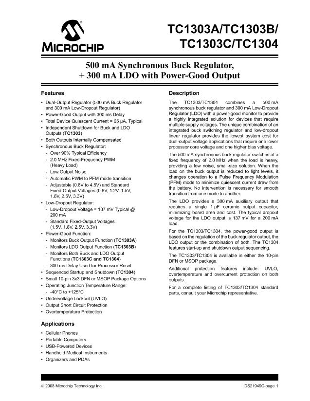
TC1303A/TC1303B/TC1303C/TC1304
DC CHARACTERISTICS (CONTINUED)
Electrical Characteristics:
V
IN1
=V
IN2
= SHDN1,2 = 3.6V, C
OUT1
= C
IN
= 4.7 µF, C
OUT2
= 1 µF, L = 4.7 µH, V
OUT1
(ADJ) = 1.8V,
I
OUT1
= 100 mA, I
OUT2
= 0.1 mA T
A
= +25°C.
Boldface
specifications apply over the T
A
range of
-40°C to +85°C.
Parameters
Output Short Circuit Current
(Average)
Wake-Up Time (From SHDN2
mode), (V
OUT2
)
Settling Time (From SHDN2
mode), (V
OUT2
)
Power-Good (PG)
Voltage Range PG
V
PG
1.0
1.2
—
89
—
—
—
140
—
5.5
5.5
96
—
—
—
—
560
V
T
A
= 0°C to +70°C
T
A
= -40°C to +85°C
V
IN
≤
2.7 I
SINK
= 100 µA
On Rising V
OUT1
or V
OUT2
V
OUTX
= V
OUT1
or V
OUT2
On Falling V
OUT1
or V
OUT2
V
OUTX
= V
OUT1
or V
OUT2
V
OUTX
= V
OUT1
or V
OUT2
Sym
I
OUTsc2
t
WK
t
S
Min
—
—
—
Typ
240
31
100
Max
—
100
—
Units
mA
µs
µs
Conditions
R
LOAD2
≤
1Ω
I
OUT1
= I
OUT2
= 50 mA
I
OUT1
= I
OUT2
= 50 mA
PG Threshold High
(V
OUT1
or V
OUT2
)
PG Threshold Low
(V
OUT1
or V
OUT2
)
PG Threshold Hysteresis
(V
OUT1
and V
OUT2
)
PG Threshold Tempco
PG Delay
PG Active Time-out Period
V
TH_H
V
TH_L
V
TH_HYS
ΔV
TH
/ΔT
t
RPD
t
RPU
94
92
2
30
165
262
% of
V
OUTX
% of
V
OUTX
% of
V
OUTX
ppm/°C
µs
ms
V
OUT1
or V
OUT2
= (V
TH
+ 100 mV)
to (V
TH
- 100 mV)
V
OUT1
or V
OUT2
= V
TH
- 100 mV
to V
TH +
100 mV,
I
SINK
= 1.2 mA
V
OUT1
or V
OUT2
= V
TH
- 100 mV
,
I
PG
= 1.2 mA V
IN2
> 2.7V
I
PG
= 100 µA, 1.0V < V
IN2
< 2.7V
V
OUT1
or V
OUT2
= V
TH
+ 100 mV
V
OUT2
≥
1.8V, I
PG
= - 500 µA
V
OUT2
< 1.8V,I
PG
= - 300 µA
PG Output Voltage Low
PG_V
OL
—
—
0.2
V
PG Output Voltage High
(TC1303B only)
Note 1:
2:
3:
4:
5:
6:
PG_V
OH
0.9* V
OUT2
—
—
V
7:
8:
The Minimum V
IN
has to meet two conditions: V
IN
≥
2.7V and V
IN
≥
V
RX
+ V
DROPOUT,
V
RX
= V
R1
or V
R2
.
V
RX
is the regulator output voltage setting.
TCV
OUT2
= ((V
OUT2max
– V
OUT2min
) * 10
6
)/(V
OUT2
* D
T
).
Regulation is measured at a constant junction temperature using low duty-cycle pulse testing. Load regulation is tested
over a load range from 0.1 mA to the maximum specified output current.
Dropout voltage is defined as the input-to-output voltage differential at which the output voltage drops 2% below its
nominal value measured at a 1V differential.
The maximum allowable power dissipation is a function of ambient temperature, the maximum allowable junction
temperature and the thermal resistance from junction to air. (i.e. T
A
, T
J
,
θ
JA
). Exceeding the maximum allowable power
dissipation causes the device to initiate thermal shutdown.
The integrated MOSFET switches have an integral diode from the L
X
pin to V
IN
, and from L
X
to P
GND
. In cases where
these diodes are forward-biased, the package power dissipation limits must be adhered to. Thermal protection is not
able to limit the junction temperature for these cases.
V
IN1
and V
IN2
are supplied by the same input source.
©
2008 Microchip Technology Inc.
DS21949C-page 9


