Typical application circuit of monolithic RF transceiver nRF401
Related component PDF download:
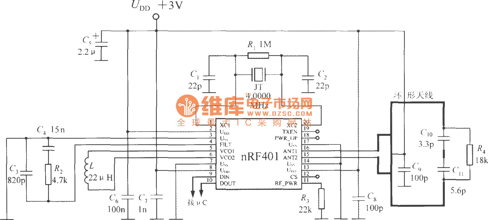
The typical application circuit of nRF401 is shown in the figure, and the UDD uses+3V power supply. The crystal oscillator circuit is composed of R1, JT, C1 and C2, and the loop filter is composed of C3, C4 and R2. R3 is the power setting resistance. C5 is power decoupling capacitance, C6 and C7 are noise elimination capacitance. The DIN and DOUT terminals are respectively connected to the TXD (serial output) and RXD (serial input) terminals of the MCU. To simplify the circuit, nRF401 can follow μ C shares a crystal oscillator circuit, as shown in the figure below. X1 and X2 are μ The crystal frequency generated from the crystal input and output of C is directly sent to the XC2 terminal of nRF401.

Related Readings
Popular Circuit Diagrams
Special Sale
